LaMeres, B.J., (2019) Quick Start Guide to Verilog (@ UB). Can also look at “Into to Logic Circuits … with Verilog”.
HDL — Hardware Description Language
In essence, it is about parallel-running functionality, and it models/describes digital circuits:
Flip Flop
CPU
adders, registers, …
There are two assignment statements: = and <=.
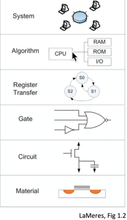
The Figure above is from the book mentioned before. It represents the different level of description / detail that occur from specification to FPGA. As we go down, we go more in detail, and as we go up we abstract more. Every component can be viewed as:
System — Specifications
Algorithm — Code, structure
Register Transfer — Logic structures
Gate — Basic gates and registers
Circuit — Electrical components
Material — Implement Electrical components
It works in a Y architecture. When you use one FPGA board, you need to map the inputs to that board. Basically, bits and maybe bytes. So the Algorithm and the Target Architecture need to be taken into consideration always together! (hence the Y idea)
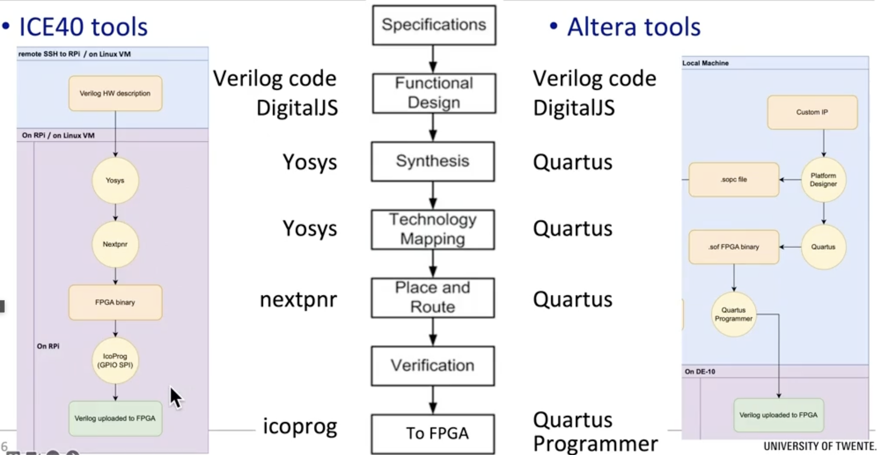
How does it work to produce FPGA code?
In this course we either use Altera tools or ICE40 tools. In Altera if you make a mistake in the number in the name or whatever, everything blows. In ICE40 you do a functional simulation (is the logic right? you can check). With icoprog you put the logic in FPGA.
It’s easier to use ICE40 tools since the coding part is only the top layer. Testing (the interface) is done through DigitalJS.
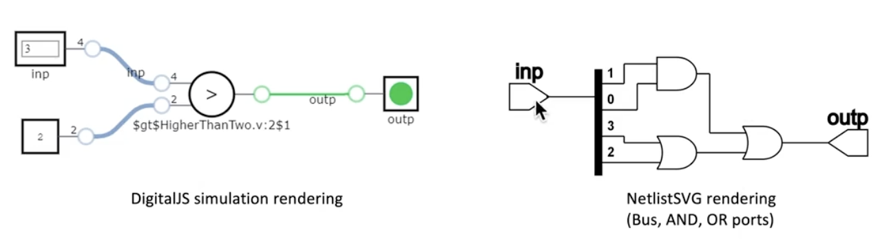
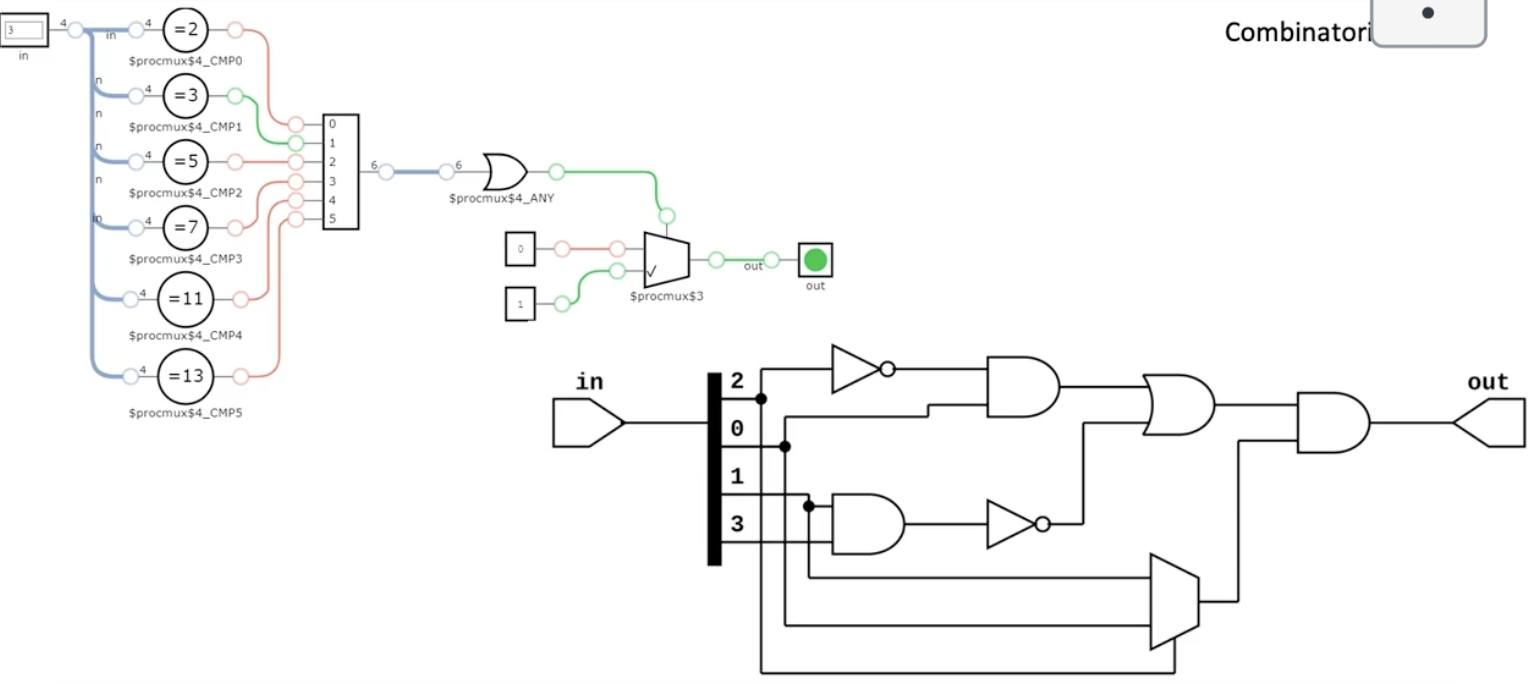
Test if number > 2
Input: a 4-bit number ⇒ values between 0-15 — input wire[3:0] inp
The left diagram I can simulate in VSCode. The flow is from left to right.
When I say I have blocking functionality, it means it runs immediately (counter-intuitive) ⇒ order of statements is important. The end-result is the current value of outp=F(inp) at that moment.
When I say I have non-blocking functionality (deferred), it means I have an event(clock)-triggered logic. The statements run concurrently and simultaneously. The end-result is all at once, synchronised on the clock.
Two assignment types
=blocking, immediately. Order matters!
<=non-blocking, synchronised on the clock. Order doesn’t matter!
NEVER EVER MIX THESE IN ONE BLOCK!!!!!
Some specifics in Verilog:
reg a = 0; // Single-bit registerb = 1; // Value HIGHc = X; // X is Unknownd = Z; // Z is floating, high impedance supported by DigitalJSinteger myNum = 531; // 32-bit vartime myTime = $time; // for simulation onlywire w = a || b; // OR gatewire z; // declare wire to assign laterassign z = w && a; // assign prev z to AND gate.reg[7:0] count = 0; // value 0..255reg[1:0] twoBit = 2 * b01; // value 1reg[3:0] arr[8]; // eight 4-bit valuesreg[3:0] q = 4'ha; // decimal value 10reg[2:0] r = 3'b110; // decimal value 6reg[2:0] s = 3'sb111; // decimal value -1"""Base: binary, octal, decimal, hexadecimalSigned base: sb, so, sd, sh"""
I need to think in digital circuits, not in C++, C, or whatever! Good thing I had a course on that in my Bachelor’s. The MSB (Most Significant Bit) is always on the left side!
Example to toggle a LED on-off every 4th count of the clock:
module TopEntity( input clk, output reg led = 0);reg[31:0]count=0; // 32 bit counteralways @(posedge clk) begin // at each positive edge of the clock do:if(count==4) begin count <= 0; // reset counter led <= ~led; // toggleend else begin count <= count+1; // incrementendendendmodule
begin … end
why 32 bits for only values of 4? makes no sense to me. Apparently, if-test is originally 99999999, (100 MHz clock). but he said we could use 2 bits.
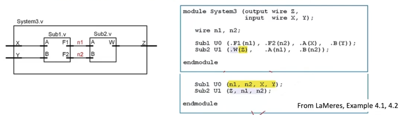
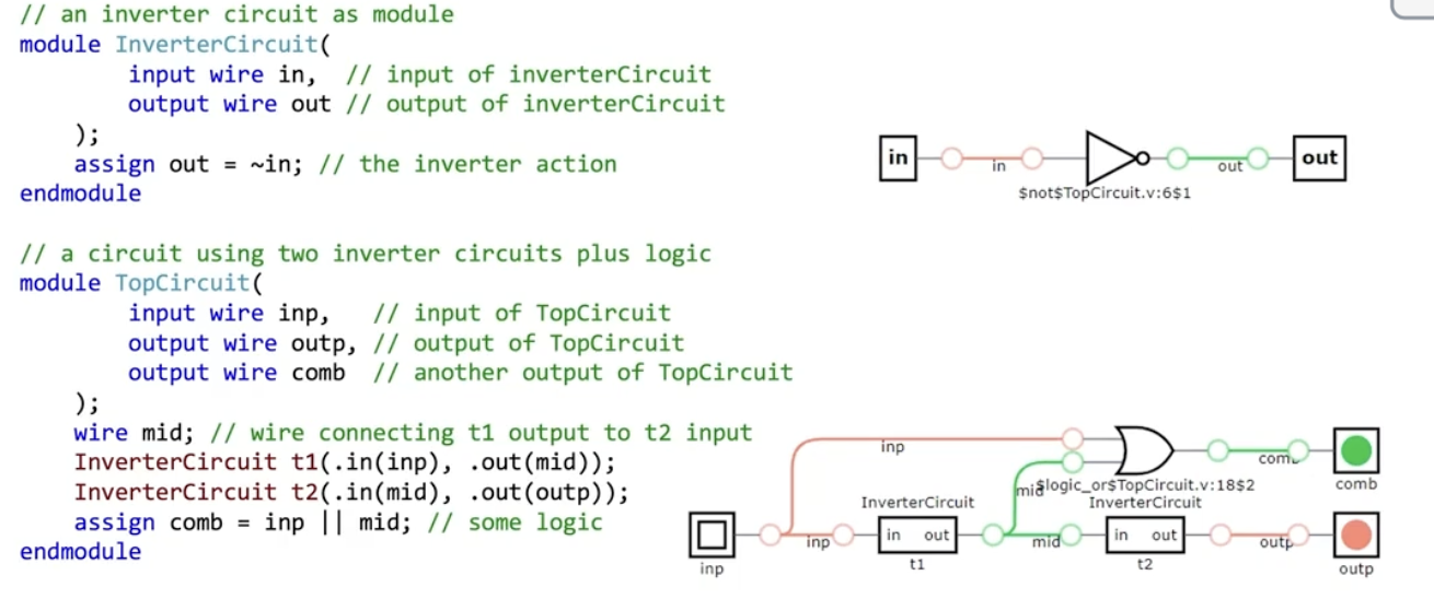
Submodules need explicit connections through wires (i.e. port mapping).
Explicit port mapping: explicitly mention submodule ports in connection list
Implicit port mapping: no submodule port names; connections must be in the same order.
We have a higher module System 3 with two sub-modules. I have to connect them; otherwise it doesn’t work. Apparently, outputs come first and inputs last. Dots I don’t know why. The lower level box I would say is the implicit; he said we should avoid it.
In the Figure below, If I click on one circle; I can see the value of that circle. Also it’s good for visualization on how to add inverter gates, OR gates, etc. Pretty fun so far.
Blocking functionality for detecting a prime input number.
module PrimeTest( input wire[3:0] in, // 4-bit num, 0..15 output wire out); always @(*) // for every input basically, execute always case(in) 2,3,5,7,11,13: out = 1; // prime default: out = 0; // not prime endcaseendmodule
I haven’t asked if indentation is necessary like in python.
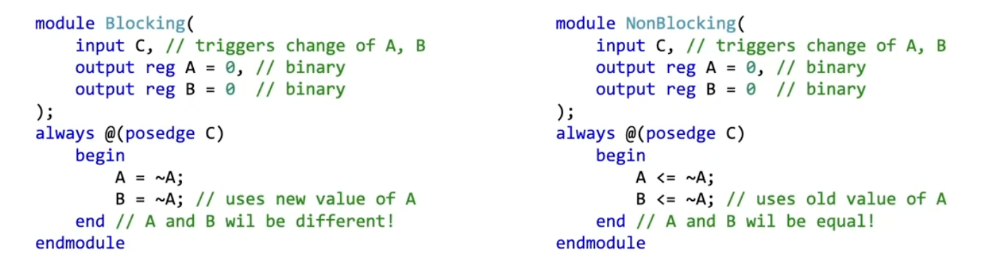
Difference in computation between BLOCKING and NON-BLOCKING
I can see only in the block we have the difference. The difference is that the Blocking one will immediately switch the values of A and B, and they will be different.
The NonBlocking will always run concurrently. So, since A does not change before B, they will both have the same value.
How to do testing?
It’s called system tasks. they can only be used in simulation, not synthesize it on FPGA. Apparently it’s not standard to always send values back from the board to the laptop. I can store the results of a simulation in a file and read complex stimulus vectors. Feels a lil bit stupid.
Text output, only at simulation
$display(); — print text(values) and newline
$write(); — print text(values) without newline
$strobe(); — display, after all simulation events are executed
$monitor(); — display, when value of the argument changes
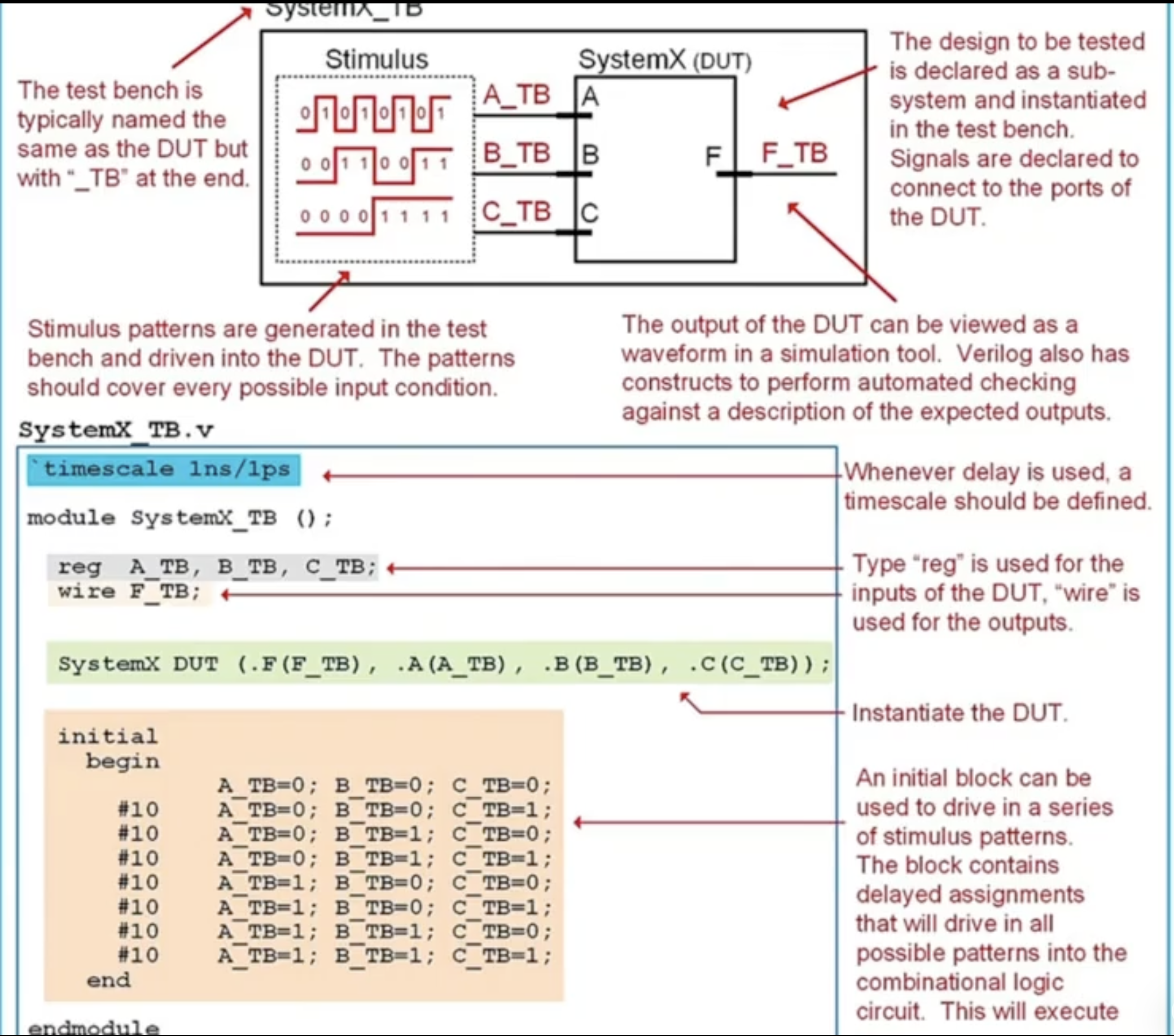
Test Bench
The device under test we already have. so we need to produce inputs and capture the outputs. Verilog provides constructs to build TBs. I did not necessarily get this part. Ok based on the Figure below I understand. Basically I need to name the Test Bench as my main system with _TB after it and declare the complex input sequence meant to test the main system.
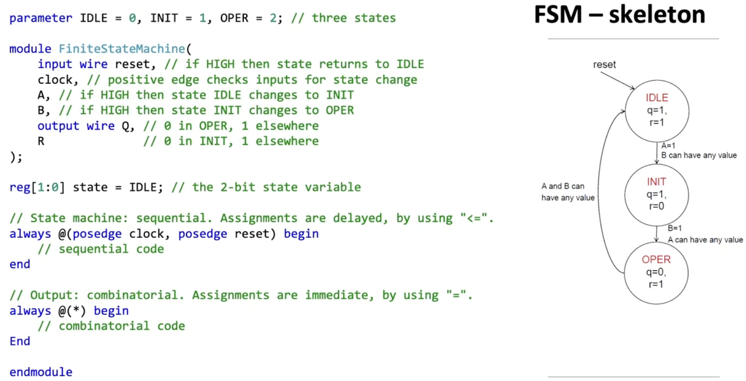
Finite State Machine
A state variable will have 2 bits. IDLE = 0, INIT = 1, OPER = 2.
Sequential process
Executed at positive edge of clock or reset, and maintains state transitions from A,B,reset. So naturally we will use <= to synchronize (i.e. delay). The order won’t matter since they run concurrently.